Tutorial on using micropositioners
Prerequisites
A decapped chip suitable for live analysis (die exposed; bond wires and pins intact). See the epoxy decapsulation tutorial page for details.
(Photos courtesy of Andrew Zonenberg unless otherwise noted.)
Procedure
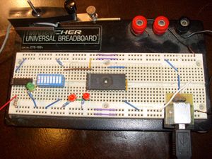
In order to do live analysis one must have a circuit to analyze. Place the chip (I used the one decapped in the epoxy decapsulation tutorial article) in a breadboard or solder it to a PCB. It is important to protect the exposed die from dust and scratches while working; I covered the opening with a glass microscope slide while building the rest of the circuit.
Items of note:
- USB power supply header at bottom right
- 74HCT04 hex inverter (configured as a buffer) to avoid drawing excessive current from die under test
- Green LED connected to probe
- DIP switches for feeding inputs to chip under test
- Signatone micropositioner at top left (probe tip not yet connected)
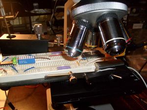
Install a tip in your micropositioner and place the circuit under the microscope. The probe tip should be hovering slightly above the die; take care not to scratch the die or knock off bond wires.
(After placing the breadboard on the microscope stage I decided to rearrange the test circuit a bit - the chip moved to the far right side in order to maintain balance. I also decided to use a different micropositioner, which seemed to fit the available space better.)
Note second micropositioner hanging off right side of breadboard. It's not hooked up to anything; I just needed a weight to help stabilize the board! A better setup is in the works.
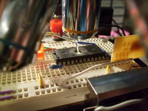
While looking through the microscope, position the probe tip over your feature of interest and lower it until it makes contact. When moving to another target be sure to raise the probe off the die; failing to do this risks breaking the probe tip, scratching the die, or both.
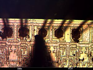
This photo was taken with the probe contacting one of the bond pads; I have so far not been able to make satisfactory contact with circuitry elsewhere on the die. Smaller probe tips (this one is 25um in size) will definitely help; the one I was using was also an old tip which may have been dulled from use.
Viewed through the microscope, it's clear that a smaller tip will be necessary to accurately probe internal structures.


